DISPLAY 101
#20 Development
| Development: The process of using a developer substance to remove a photoresist after its exposure to light to create the desired pattern on the TFT. |
Let’s take a look at the next stage of the photolithography process, Development. Development is the process of removing the photoresist (PR) after everything has been exposed to light. Especially at this stage, it is somewhat similar to how photographs are developed. After this process, only the desired shape is left on the TFT substrate so that the circuit pattern can be generated in the next step, Etching.
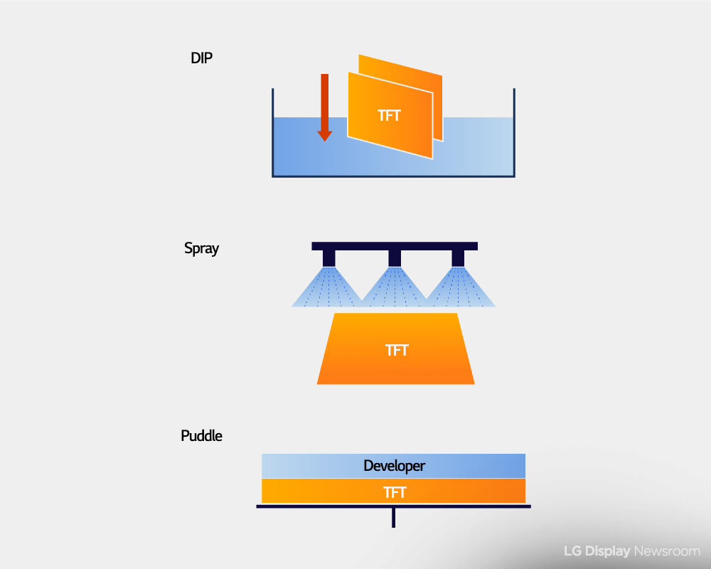
Various methods of applying developer

| Method of applying developer | Concept |
| Dip | Development by immersing the substrate in a developer bath |
| Spray | Spray developer onto the substrate with a nozzle |
| Puddle | Apply developer onto the substrate where it stays due to surface tension |
As mentioned in the previous article, there are two types of PR, positive and negative. With a positive PR, the areas that are exposed to light change chemical structure so that it becomes easier to wash them away with a developer. When these areas are exposed to developer, they are eliminated. With a negative PR, the areas exposed to light harden and remain, and the areas that were not exposed to light are removed with a developer.
There are several methods used to apply the developer to the substrate. The first is the Dip method, where the substrate is dipped into a bath of developer. The second is the Spray method, in which the developer is sprinkled onto the substrate through nozzles. The third is the Puddle method, in which developer is allowed to fully coat the substrate and its surface tension is used to keep everything together. The most efficient method is based on a number of complex factors, such as exposure time, developer temperature, and development time.


